A first photo on mainline Linux

 Cameras on phones have gotten so good that they are often taken for granted. They are expected to always work and produce good quality photos with fairly accurate colors. Those trying to make them work on a Linux phone for the first time would not have it as easy though, as they get to discover the several components involved in long complicated processes to arrive at a ready-to-use JPEG image. This is why cameras remain one of, if not the least supported feature of all Linux phones, whether originally made to run Linux or had it ported to them.
To find out how it all works, an attempt is made to enable the main camera on a Xiaomi Mi Note 2 on mainline Linux.
Understanding the hardware
What the average end-user might know about this phone is that it has a Sony IMX318 main camera with a native resolution of 5488x4112 adding up to 22.56 MP. Some might also know that the SoC on the phone, the Qualcomm Snapdragon 821, has an ISP – short for Image Signal Processor – that helps with processing photos. To enable the camera on Linux for the first time would require a much lower-level understanding of the hardware, however. A quick look at the schematics of this phone would be a good way to begin.
Searching for “camera” shows a few interesting blocks. This one labeled REAR CAMERA seems like a good starting point:
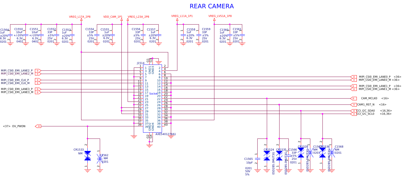 This show several lines coming out of a socket, which the camera module presumably plugs into. Starting with the obvious, there are a few lines going up. These are rails that supply power to the camera module.
 CAM_MCLK0 must be a clock, and CAM1_RST_N a reset line. As for data, two categories of lines can be seen: One with the CCI_I2C prefix, and another with MIPI_CSI. CCI, or Camera Control Interface, is just an I2C bus dedicated to controlling the camera module. Since I2C has quite a low bandwidth, it would not be adequate to carry image data from the sensor, hence the use of the MIPI Camera Serial Interface. MIPI CSI is a high bandwidth serial bus designed specifically for transferring image data from cameras.
Another block labeled FRONT CAMERA is also shown in the schematic diagram:
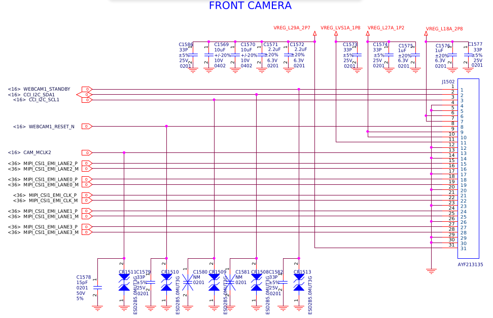 It shows a similar setup, with some power rails, a clock line, a reset line, as well as CCI and CSI lines.
A closer look at the camera module
A camera module consists of an image sensor that collects light and outputs signals to recreate the image digitally, as well as a lens to focus light falling on the sensor. Depending on the camera module, there can also be an actuator that physically moves the lens to change the focus distance. Many camera modules found on phones these days have multiple sets of sensors and lenses with different focal lengths for added flexibility. The main camera on the Mi Note 2 – as mentioned previously – has a Sony IMX318 image sensor. This camera can also change focus distance both automatically and manually, so it must have a lens actuator. The image sensor is the most important part of the operation, so it will be the focus target*.
Documentation would become necessary to learn more about the image sensor. To write a driver for the sensor would of course require at least a register map with definitions, which is sometimes included in the datasheet, or found in a separate Technical Reference Manual or Functional Specification. Unfortunately, there are no publicly available documents to be found, other than a product description including general specifications of the sensor.
With this phone originally running Android, the downstream kernel can be taken as an alternative source of information. In this case however, the vendor decided to use a proprietary userspace driver, meaning there is no source code showing how the sensor is controlled.
Dead end?
Having no documentation, will the camera require yet another reverse engineering effort? We must go deeper.
Having a proprietary driver for the camera on this phone does not necessarily mean that it is done similarly in other phones, so there might be an open source kernel driver in another downstream kernel for a different device. Searching for “IMX318” across GitHub reveals a couple of drivers, one belonging to a NVIDIA Jetson Nano kernel, and the other to some common MediaTek MT6757 kernel.
Before looking at the downstream drivers however, it would be better to take a look at an existing mainline driver for a similar sensor to gain a general understanding of how these drivers are constructed, and figure out what needs to be known to write a new one. I2C-controlled camera sensor drivers are located in drivers/media/i2c. Here, several drivers for Sony sensors are found, distingushed by the imx prefix in their names.
A look at an existing driver
Almost every Linux driver starts at a probe function where all necessary initialization steps are made to prepare the hardware for operation, as well as to register the driver to the relevant kernel subsystems. Looking at the IMX214 driver, the general flow of events goes like this:
- The device tree node is first parsed, endpoints are identified and link frequency compatibility is tested:
  ret = imx214_parse_fwnode(dev);
      if (ret)
          return ret;
static int imx214_parse_fwnode(struct device *dev) { struct fwnode_handle *endpoint; struct v4l2_fwnode_endpoint bus_cfg = { .bus_type = V4L2_MBUS_CSI2_DPHY, }; unsigned int i; int ret; endpoint = fwnode_graph_get_next_endpoint(dev_fwnode(dev), NULL); if (!endpoint) { dev_err(dev, "endpoint node not found\n"); return -EINVAL; } ret = v4l2_fwnode_endpoint_alloc_parse(endpoint, &bus_cfg); if (ret) { dev_err(dev, "parsing endpoint node failed\n"); goto done; } for (i = 0; i < bus_cfg.nr_of_link_frequencies; i++) if (bus_cfg.link_frequencies[i] == IMX214_DEFAULT_LINK_FREQ) break; if (i == bus_cfg.nr_of_link_frequencies) { dev_err(dev, "link-frequencies %d not supported, Please review your DT\n", IMX214_DEFAULT_LINK_FREQ); ret = -EINVAL; goto done; } done: v4l2_fwnode_endpoint_free(&bus_cfg); fwnode_handle_put(endpoint); return ret; } - The external clock is located and configured:
imx214->xclk = devm_clk_get(dev, NULL); if (IS_ERR(imx214->xclk)) { dev_err(dev, "could not get xclk"); return PTR_ERR(imx214->xclk); } ret = clk_set_rate(imx214->xclk, IMX214_DEFAULT_CLK_FREQ); if (ret) { dev_err(dev, "could not set xclk frequency\n"); return ret; } - Regulators and GPIOs are parsed:
ret = imx214_get_regulators(dev, imx214); if (ret < 0) { dev_err(dev, "cannot get regulators\n"); return ret; } imx214->enable_gpio = devm_gpiod_get(dev, "enable", GPIOD_OUT_LOW); if (IS_ERR(imx214->enable_gpio)) { dev_err(dev, "cannot get enable gpio\n"); return PTR_ERR(imx214->enable_gpio); } - A V4L2 subdevice is initialized,
v4l2_i2c_subdev_init(&imx214->sd, client, &imx214_subdev_ops);and its controls are configured:
v4l2_ctrl_handler_init(&imx214->ctrls, 3); imx214->pixel_rate = v4l2_ctrl_new_std(&imx214->ctrls, NULL, V4L2_CID_PIXEL_RATE, 0, IMX214_DEFAULT_PIXEL_RATE, 1, IMX214_DEFAULT_PIXEL_RATE); imx214->link_freq = v4l2_ctrl_new_int_menu(&imx214->ctrls, NULL, V4L2_CID_LINK_FREQ, ARRAY_SIZE(link_freq) - 1, 0, link_freq); if (imx214->link_freq) imx214->link_freq->flags |= V4L2_CTRL_FLAG_READ_ONLY; imx214->exposure = v4l2_ctrl_new_std(&imx214->ctrls, &imx214_ctrl_ops, V4L2_CID_EXPOSURE, 0, 3184, 1, 0x0c70); imx214->unit_size = v4l2_ctrl_new_std_compound(&imx214->ctrls, NULL, V4L2_CID_UNIT_CELL_SIZE, v4l2_ctrl_ptr_create((void *)&unit_size)); ret = imx214->ctrls.error; if (ret) { dev_err(&client->dev, "%s control init failed (%d)\n", __func__, ret); goto free_ctrl; } imx214->sd.ctrl_handler = &imx214->ctrls; mutex_init(&imx214->mutex); imx214->ctrls.lock = &imx214->mutex; - Then finally a media entity is configured and the V4L2 subdevice is registered:
  imx214->sd.flags |= V4L2_SUBDEV_FL_HAS_DEVNODE;
  imx214->pad.flags = MEDIA_PAD_FL_SOURCE;
  imx214->sd.dev = &client->dev;
  imx214->sd.entity.function = MEDIA_ENT_F_CAM_SENSOR;

  ret = media_entity_pads_init(&imx214->sd.entity, 1, &imx214->pad);
  if (ret < 0) {
      dev_err(dev, "could not register media entity\n");
      goto free_ctrl;
  }

  imx214_entity_init_cfg(&imx214->sd, NULL);

  ret = v4l2_async_register_subdev_sensor(&imx214->sd);
  if (ret < 0) {
      dev_err(dev, "could not register v4l2 device\n");
      goto free_entity;
  }
Infrastructure
These steps show some basic elements the sensor needs, namely clocks and regulators. The sensor takes in one clock signal and uses it internally to generate all clock signals it needs to function. This is shown as xclk (short for external clock) in the driver. A second clock that is part of the MIPI CSI bus is used to synchronize the CSI links, the frequency of which is referred to as link frequency in the driver. The frequency read from the device tree must be supported by the sensor, hence the compatibility checking. Link frequency will become important later.
As for power, the sensor needs three supplies: one to power the digital part of the IC, one to power its analog part, and one to pull-up I/O lines.
V4L2
Short for Video for Linux version 2, V4L2 is a Linux API for managing video devices of all kinds, including codecs, TV tuners, multiplexers and of course, cameras. It allows for dealing with complicated devices as sets of simpler subdevices, each having its own controls, as well as source and sink pads to link it with other subdevices and control the flow of data through a pipeline. The kernel side of V4L2 is used throughout the sensor driver.
Back to the IMX318
The first thing to do would be to power on the sensor. To do so, the power rails it is hooked up to must be brought up, the external clock must be enabled and set to a suitable frequency, and the reset line must be asserted then deasserted to reset the sensor. It might seem simple at first, but as it would turn out later, it needs to be done in a specific way in order to get the sensor into a working state.
A good first step to find the correct power on sequence would be to see how the stock driver does it. Although the vendor decided to use a proprietary blob to drive the sensor, the kernel remains open-source, and anything regarding clocks, regulators or GPIOs goes through it at some point. Conveniently, they decided to have the userspace driver give the kernel instructions on a power sequence which it would then execute. Even more so, the parsing and execution of the instructions happens in a single function named msm_camera_power_up. It even has dynamic debug messages that if enabled, would allow for monitoring of the power on process as it happens. This function calls msm_cam_sensor_handle_reg_gpio for enabling regulators, so debug messages must be enabled there too. Once all relevant messages are enabled, the sequence can be seen in the kernel log:
[   12.194390] msm_camera_power_up:1538
[   12.194989] msm_camera_power_up index 0
[   12.194994] msm_camera_power_up type 1
[   12.194998] msm_camera_power_up:1607 gpio set 86 val 0
[   12.196751] msm_camera_power_up index 1
[   12.196758] msm_camera_power_up type 1
[   12.196761] msm_camera_power_up:1607 gpio set 30 val 0
[   12.198801] msm_camera_power_up index 2
[   12.198808] msm_camera_power_up type 2
[   12.199424] msm_cam_sensor_handle_reg_gpio: 1420 Seq val: 2, config: 1
[   12.199429] msm_cam_sensor_handle_reg_gpio: 1454 GPIO offset: 4, seq_val: 2
[   12.199433] msm_camera_power_up index 3
[   12.199435] msm_camera_power_up type 2
[   12.199888] msm_cam_sensor_handle_reg_gpio: 1420 Seq val: 0, config: 1
[   12.199892] msm_cam_sensor_handle_reg_gpio: 1454 GPIO offset: 5, seq_val: 0
[   12.199895] msm_camera_power_up index 4
[   12.199898] msm_camera_power_up type 2
[   12.201948] msm_cam_sensor_handle_reg_gpio: 1420 Seq val: 1, config: 1
[   12.201954] msm_cam_sensor_handle_reg_gpio: 1454 GPIO offset: 3, seq_val: 1
[   12.201960] msm_camera_power_up index 5
[   12.201963] msm_camera_power_up type 2
[   12.202577] msm_cam_sensor_handle_reg_gpio: 1420 Seq val: 3, config: 1
[   12.202582] msm_cam_sensor_handle_reg_gpio: 1454 GPIO offset: 6, seq_val: 3
[   12.202587] msm_camera_power_up index 6
[   12.202590] msm_camera_power_up type 0
[   12.203887] msm_camera_power_up index 7
[   12.203894] msm_camera_power_up type 1
[   12.203898] msm_camera_power_up:1607 gpio set 86 val 2
[   12.205735] MSM-CPP cpp_init_hardware:1011 CPP HW Version: 0x60000000
[   12.205745] MSM-CPP cpp_init_hardware:1029 stream_cnt:0
[   12.214102] msm_camera_power_up index 8
[   12.214109] msm_camera_power_up type 1
[   12.214113] msm_camera_power_up:1607 gpio set 30 val 2
[   12.219075] msm_pm_qos_update_request: update request -1
[   12.219080] msm_pm_qos_add_request: add request
[   12.225387] msm_cci_init:1434: hw_version = 0x10040000
[   12.225466] msm_camera_power_up exit
This might look like a lot at first glance, but it basically does the following:
- Set GPIO 86 to LOW,
- Set GPIO 30 to LOW,
- Enable VANA supply,
- Enable VDIG supply,
- Enable VI/O supply,
- Enable VAF supply,
- Enable external clock,
- Set GPIO 86 to HIGH,
- Set GPIO 30 to HIGH.
Supplies are found using the GPIO offset values shown in the msm_cam_sensor_handle_reg_gpio messages, which correspond to entries in an enum defined in a separate header file.
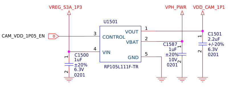
Looking at schematics, GPIO 30 is found to be the CAM1_RST_N reset pin seen before:
 The
The _N suffix suggests that it is active low, which is to say that it is asserted by setting it to LOW, and deasserted by setting it to HIGH.
As for GPIO 86, its name suggests that it is an enable pin of a regulator:
 Following it, we end up at what seems to be a LDO (short for Low-Dropout Regulator):
With the GPIOs figured out, now come regulators, which can be found in downstream DTS:
cam_vdig-supply = <&pm8994_s3>;
cam_vio-supply = <&pm8994_lvs1>;
cam_vana-supply = <&pm8994_l17>;
cam_vmipi-supply = <&pm8994_l11>;
qcom,cam-vreg-name = "cam_vdig", "cam_vio", "cam_vana", "cam_vmipi";
VAF supply can be found separately in the actuator node
cam_vaf-supply = <&pm8994_l23>;
qcom,cam-vreg-name = "cam_vaf";
There does not seem to be any references to the LDO found in schematics earlier. However, when looking closely, it can be noticed that VDIG supply is the same as VIN of the LDO. This would suggest that VDIG is actually the LDO output rather than S3 of the PM8994 PMIC. In fact, this pattern is frequently seen in the downstream kernel, where an LDO (or any kind of external regulator with fixed voltage output and an enable pin) is not described in DTS, and its enable pin is treated as if it were of the component the regulator supplies power to.
Finally, the external clock and its frequency are also found in downstream DTS:
clocks = <&clock_mmss clk_mclk0_clk_src>,
		<&clock_mmss clk_camss_mclk0_clk>;
clock-names = "cam_src_clk", "cam_clk";
qcom,clock-rates = <24000000 0>;
Putting all of this together, the power sequence would look like this:
- Disable VDIG supply,
- Assert reset
- Enable VANA supply,
- Enable parent supply of VDIG supply,
- Enable VI/O supply,
- Enable VAF supply,
- Enable external clock and set it to 24MHz,
- Enable VDIG supply,
- Deassert reset.
This sequence would prove to be ineffective, however. Fortunately, there is source code to refer to in this case: The driver from the Jetson Nano kernel. This driver’s power on function suggests adding a 19ms delay after deasserting reset.
Combining information from the sequence captured on the running downstream kernel and the driver in the Jetson Nano kernel tree, and after some experimentation, a working power on function is made:
static int imx318_power_on(struct device *dev)
{
	struct i2c_client *client = to_i2c_client(dev);
	struct v4l2_subdev *sd = i2c_get_clientdata(client);
	struct imx318 *imx318 = to_imx318(sd);
	int ret;

	gpiod_set_value_cansleep(imx318->reset_gpio, 1);

	ret = regulator_bulk_enable(IMX318_NUM_SUPPLIES, imx318->supplies);
	if (ret) {
		dev_err(imx318->dev, "Failed to enable regulators: %d\n", ret);
		regulator_bulk_disable(IMX318_NUM_SUPPLIES, imx318->supplies);
		return ret;
	}

	ret = clk_prepare_enable(imx318->extclk);
	if (ret < 0) {
		dev_err(imx318->dev, "Failed to enable external clock: %d\n", ret);
		return ret;
	}

	gpiod_set_value_cansleep(imx318->reset_gpio, 0);

	/* Wait for sensor to power on */
	usleep_range(19000, 20000);

	dev_dbg(imx318->dev, "Powered on\n");

	return ret;
}
Sensor initialization
The sensor has to be initialized first before it can capture any images. There are many registers in the sensor that are written to during initialization, some of which are related to the internal clock tree, while others configure image properties, timing, and so on.
Ideally, each of those registers should be labeled clearly in the driver, then written to individually with also clearly labeled values, or if a bitmask, constructed at the time of writing. However, due to lack of documentation, and sometimes simply due to the sheer number of registers that need to be written, many sensor drivers just have a bunch of magic numbers arranged in tables of register-value pairs, which then get applied as needed. Going back to the downstream drivers found previously, such register tables can be seen. In the Jetson Nano driver, the tables are placed in a separate header file, while in the MT6757 driver, they are placed in the source file of the driver.
In both drivers, there is a common table that is quite long, and a few smaller mode tables. The common table is used once for initialization, while the mode tables are used to switch between, well, different modes.
Modes?
While the IMX318 sensor has a native resolution of 5488x4112, it can also operate at other resolutions with various refresh rates. The combination of resolution and refresh rate* is referred to as a mode.
Due to the difference in bits per image and the number of images that need to be transmitted per second for each mode, The rate at which the sensor has to transmit signals depends on the mode configured. This is where link frequency comes in. Theoretically speaking, the minimum link frequency of a MIPI CSI bus required at a certain mode can be calculated as follows:
\[f = {whbr \over 2n}\]Where:
- \(f\): Link frequency;
- \(w\): Image width;
- \(h\): Image height;
- \(b\): Bit depth (bits per pixel);
- \(r\): Refresh rate; and
- \(n\): CSI link count.
The MIPI CSI bus operates with double data rate (or DDR for short). This means that two bits are transferred every clock cycle, one on the rising edge, and another on the falling edge:
Furthermore, the bus may consist of multiple links, each transmitting bits separately. These two facts make us arrive at the denominator \(2n\) shown in the equation above, meaning two bits per link transferred in a clock cycle. Meanwhile, the numerator is the number of bits that need to be transferred every second: The number of pixels in an image (\(w*h\)) times the number of bits per pixel (\(b\)), multiplied by the number of images transferred each second (\(r\)).
Formats
An image can be digitally represented in countless ways. The method used to arrange image data into a sequence of bytes is known as an image format. Before looking into formats, it would help to understand how image sensors are constructed.
To put simply, image sensors – like displays – have pixels, lots of pixels, in a grid array. While a display emits light from its pixels, image sensors detect it. Displays usually have subpixels within each pixel, each emitting one of the additive primary colors (red - green - blue). However, image sensors do not have subpixels, but rather a different color filter on each pixel in a certain pattern known as a Bayer filter. While this makes every pixel only sensitive* to one of the primary colors, it is possible to achieve a full color image by interpolating color values from neighboring pixels for each pixel.
The Sony IMX318 sensor, like many other Sony image sensors used on phones, has a 10-bit RGGB bayer format. This means that each pixel has a 10-bit value, and that a 2x2 grid has red, green, green then blue pixels left to right, top to bottom:
Coming back to the bit depth, one might wonder how pixel values are stored in bytes, considering that each pixel has 10 bits while a byte only has 8. The easiest way would be to just store each pixel value in two bytes (numbers represent pixel indices, X represents unused bits):
00000000 00XXXXXX 11111111 11XXXXXX 22222222 22XXXXXX 33333333 33XXXXXX
This is known as an unpacked 10-bit format. This method is quite inefficient though; as it leaves many bits unused. Due to that, it is rarely used outside of processing stages, where the data would likely need to be unpacked anyway.
A much efficient method to handle 10-bit pixel values is to use a packed 10-bit format, in which the bits from 4 pixels (\(4 * 10 = 40\)) fit perfectly into 5 bytes (\(5 * 8 = 40\)). It may sound logical at first to pack the bits sequencially, where bits in a row of 4 pixels would be placed in sequence like this:
00000000 00111111 11112222 22222233 33333333
But as it turns out, the bits are usually packed like this:
00000000 11111111 22222222 33333333 00112233
While this may look strange, it is actually a clever way of packing 10-bit pixel values into bytes. In this arrangement, the eight most significant bits of the values are stored in the first 4 bytes, while the two least significant bits of every value are put together in the fifth byte. This allows for converting a 10-bit image into an 8-bit one by simply discarding every fifth byte in the sequence, leaving only the most significant bits behind. This feature will help with decoding raw sensor data later.
Putting everything together
With all necessary elements found, it is now possible to assemble a functional driver for the IMX318 sensor.
Device tree
To bring the driver to life, it is necessary to describe the camera hardware in the device tree.
To begin with, the camera subsystem is enabled, and its analog supply is specified:
&camss {
	status = "okay";

	vdda-supply = <&vreg_l2a_1p25>;
};
The analog supply can be found throughout the downstream device tree in the qcom,mipi-csi-vdd-supply property.
The CCI block of the camera subsystem is also enabled:
&cci {
	status = "okay";
};
A node for the VDIG supply LDO is added under the root node:
/ {
	vdd_cam_1p1: vdd-cam-1p1 {
		compatible = "regulator-fixed";
		regulator-name = "vdd_cam_1p1";
		regulator-min-microvolt = <1100000>;
		regulator-max-microvolt = <1100000>;
		vin-supply = <&vreg_s3a_1p3>;
		regulator-allow-set-load;

		gpio = <&tlmm 86 0>;
		enable-active-high;
		pinctrl-names = "default";
		pinctrl-0 = <&vdd_cam_1p1_default>;
	};
};
Along with a pin state for its enable pin in the tlmm node (GPIO controller of the SoC):
&tlmm {
	vdd_cam_1p1_default: vdd_cam_1p1_default {
		pins = "gpio86";
		function = "gpio";
		drive-strength = <16>;
		bias-disable;
	};
};
Now, the sensor can be added to the node of the CCI bus it is connected to:
&cci_i2c0 {
	clock-frequency = <1000000>;

	/* Rear camera */
	camera-sensor@1a {
		compatible = "sony,imx318";
		reg = <0x1a>;

		vana-supply = <&vreg_l17a_2p8>;
		vio-supply = <&vreg_lvs1a_1p8>;
		vmipi-supply = <&vreg_l11a_1p1>;
		vdig-supply = <&vdd_cam_1p1>;

		reset-gpios = <&tlmm 30 GPIO_ACTIVE_LOW>;

		clocks = <&mmcc CAMSS_MCLK0_CLK>;
		clock-frequency = <24000000>;
	};
};
Here, all needed supplies, clocks, GPIOs are listed, all of which were found previously. The clock frequency of the CCI bus is also configured. The address of the sensor (as seen in the node name and the reg property) is found by setting a random address at first then running i2cdetect on this CCI bus after the driver is probed and the power on sequence is executed.
Pin states for the reset and clock pins of the sensor are also added to tlmm node:
&tlmm {
	cam_sensor_rear_default: cam_sensor_rear_default {
		pins = "gpio30";
		function = "gpio";
		drive-strength = <2>;
		bias-disable;
	};

	cam_sensor_rear_sleep: cam_sensor_rear_sleep {
		pins = "gpio30";
		function = "gpio";
		drive-strength = <2>;
		bias-pull-up;
	};

	mclk0_default: mclk0_default {
		pins = "gpio13";
		function = "cam_mclk";
		drive-strength = <2>;
		bias-disable;
	};

	mclk0_sleep: mclk0_sleep {
		pins = "gpio13";
		function = "gpio";
		drive-strength = <2>;
		bias-pull-down;
	};
};
function = "cam_mclk" is needed for GPIO 13 to make it output a clock signal for the camera rather than functioning as a regular GPIO.
So far, the camera subsystem has been enabled and the image sensor added, but they have not been linked together. To do so, endpoints – as seen before in the IMX214 driver – are used. An endpoint is described in the sensor node:
&cci_i2c0 {
	camera-sensor@1a {
		port {
			imx318_ep: endpoint {
				data-lanes = <0 1 2 3>;
				link-frequencies = /bits/ 64 <211562400 693600000 846249600>;
				remote-endpoint = <&csiphy0_ep>;
			};
		};
	};
};
Here, CSI data lanes used and supported link frequencies are specified. The equation shown previously is used to calculate those frequencies based on modes supported by the driver. Finally, the endpoint at the other end of the communication channel is specified. In this case, the CSI physical layer lies at the other end of the CSI bus.
Likewise, an endpoint is descibed in the camera subsystem node:
&camss {
	ports {
		port@0 {
			reg = <0>;
			csiphy0_ep: endpoint {
				clock-lanes = <7>;
				data-lanes = <0 1 2 3>;
				remote-endpoint = <&imx318_ep>;
			};
		};
	};
};
Used data lanes are also specified here, as well as the physical index of the clock lane. The remote-endpoint property is used here too, this time pointing towards the sensor endpoint.
With that done, it is time to put the image sensor to use.
Getting data out of the sensor
Now that we have a driver, the sensor can be instructed to start capturing images (or frames) and transmitting them over the MIPI CSI bus. However, we still cannot get the data it outputs; as it has to get through the SoC camera pipeline.
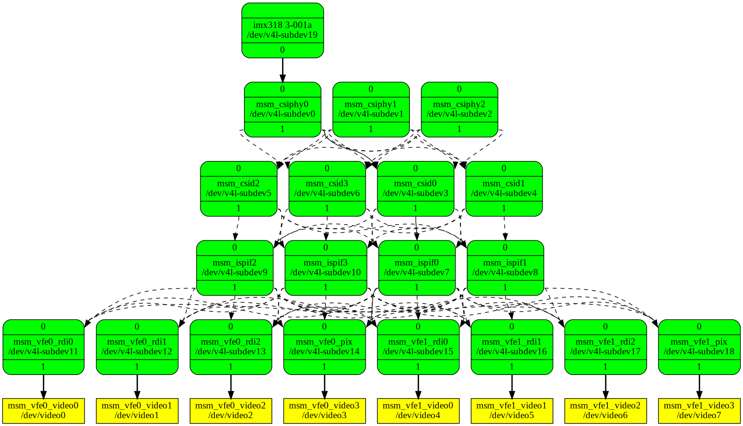
The MSM8996 SoC has a camera subsystem (abbreviated to CAMSS as seen before) with several stages, starting at the CSI physical layer (CSIPHY) which brings in electrical signals from outside the SoC, going through the CSI decoder (CSID) which decodes data carried in those signals, then the ISP interface (ISPIF) which provides access to the ISP for processing, arriving finally at the video frontend (VFE) at which image data is exported from the camera subsystem to other parts of the SoC by pixel interface (PIX) and raw dump interface (RDI) blocks. A great blog post by Linaro, as well as the Linux Kernel Documentation explain this in more detail.
In order to retrieve data from the sensor, all of these stages must be configured and linked together. The media-ctl tool can be used for that. First, the stages are linked together:
# media-ctl -d /dev/media0 -l '"msm_csiphy0":1->"msm_csid0":0[1],"msm_csid0":1->"msm_ispif0":0[1],"msm_ispif0":1->"msm_vfe0_rdi0":0[1]'
A visual representation can be obtained with the same tool, with solid lines showing established links, and dashed lines showing possible ones:
$ media-ctl --print-dot | dot -Tpng
Then, source and sink pads of all stages are configured to a certain image format:
# media-ctl -d /dev/media0 -V '"imx318 3-001a":0[fmt:SRGGB10_1X10/3840x2160 field:none],"msm_csiphy0":0[fmt:SRGGB10_1X10/3840x2160 field:none],"msm_csid0":0[fmt:SRGGB10_1X10/3840x2160 field:none],"msm_ispif0":0[fmt:SRGGB10_1X10/3840x2160 field:none],"msm_vfe0_rdi0":0[fmt:SRGGB10_1X10/3840x2160 field:none]'
Now the pipeline is ready to start streaming, which is to say begin capturing frames from the sensor and passing them through the rest of the pipeline until they reach memory where they can be accessed. v4l2-ctl is used to capture a single frame:
# v4l2-ctl -d /dev/video0 --set-fmt-video=width=3840,height=2160,pixelformat='pRAA' --stream-mmap --stream-to=img --stream-count=1 --verbose

VIDIOC_QUERYCAP: ok
VIDIOC_G_FMT: ok
VIDIOC_S_FMT: ok
Format Video Capture Multiplanar:
	Width/Height      : 3840/2160
	Pixel Format      : 'pRAA' (10-bit Bayer RGRG/GBGB Packed)
	Field             : None
	Number of planes  : 1
	Flags             :
	Colorspace        : sRGB
	Transfer Function : sRGB
	YCbCr/HSV Encoding: ITU-R 601
	Quantization      : Full Range
	Plane 0           :
	   Bytes per Line : 4800
	   Size Image     : 10368000
		VIDIOC_REQBUFS returned 0 (Success)
		VIDIOC_QUERYBUF returned 0 (Success)
		VIDIOC_QUERYBUF returned 0 (Success)
		VIDIOC_QUERYBUF returned 0 (Success)
		VIDIOC_QUERYBUF returned 0 (Success)
		VIDIOC_QBUF returned 0 (Success)
		VIDIOC_QBUF returned 0 (Success)
		VIDIOC_QBUF returned 0 (Success)
		VIDIOC_QBUF returned 0 (Success)
		VIDIOC_STREAMON returned 0 (Success)
Now we have a file named img that contains raw data captured from the sensor.
Processing data into a viewable image
To get an actual image would require processing the captured sensor data first. The easy part would be to convert pixels into 8-bit depth thanks to the packed 10-bit format. However, due to the bayer filter used on the sensor, getting proper color values at capture resolution would require interpolating values of several pixels in a process called demosaicing. A much easier way to get an image however would be to treat every 4 pixels in a 2x2 square grid as subpixels of a single bigger pixel. This will effectively result in an image with 1/4 the capture resolution, but for testing purposes that would still be more than enough. Putting all of this in a Python script:
import sys
from PIL import Image

width = 3840
height = 2160
# Each group of 4 pixels is 5 bytes long
line_length = width * 5 // 4

f = open(sys.argv[1], "rb")
data = f.read()

# Preview image will have 1/2 the dimensions, 1/4 the resolution
preview_img = Image.new("RGB", (width // 2, height // 2))
preview_pixels = preview_img.load()

x = 0
y = 0
pixel = [0, 0, 0]

for y in range(height // 2):
	for x in range(width // 2):
		# Index of top-left corner of pixel in original array
		i = x * 2
		# Skip 5th bytes to get 8-bit pixels
		i += (i+1) // 4

		# Red
		pixel[0] = data[(y*2) * line_length + i]

		# Green
		pixel[1] = data[(y*2) * line_length + i+1]
		# Average value of second green pixel with first one
		pixel[1] += data[(y*2+1) * line_length + i]
		pixel[1] //= 2

		# Blue
		pixel[2] = data[(y*2+1) * line_length + i+1]

		preview_pixels[x, y] = (pixel[0], pixel[1], pixel[2])

preview_img.save("img.png")
And finally, after some manual adjustments:
The Mi Note 2 is starting to open its eye...
— Yassine Oudjana (@y_oudjana) December 16, 2021
First image ever taken while running the mainline Linux kernel, with a fully open-source camera stack from the camera sensor and SoC camera subsystem drivers to the userspace tools. pic.twitter.com/JfB1P8yrK2

Next steps
While getting the camera sensor to work on mainline Linux at all is a great achievement, it is quite useless if the images it captures are underexposed, have inaccurate colors and are out of focus. In order to achieve proper camera support, at least a few things must be taken care of:
- Gain and exposure controls must be added to the sensor driver. Part of this has already been done at the time of writing.
- The lens actuator needs to be enabled as well. This has also been done. Auto-focus has not been implemented yet, however.
- Some color calibration data must be collected to post-process the raw data coming out of the sensor.
For now, mostly unprocessed images can be captured using Megapixels.